Sapphire Ingot Growth Equipment Czochralski CZ Method para sa Pagprodyus og 2inch-12inch Sapphire Wafers


Prinsipyo sa Pagtrabaho
Ang CZ nga pamaagi naglihok pinaagi sa mosunod nga mga lakang:
1. Pagtunaw sa Hilaw nga Materyal: Taas nga kaputli Al₂O₃ (kaputli>99.999%) natunaw sa usa ka iridium crucible sa 2050–2100°C.
2. Seed Crystal Introduction: Ang binhi nga kristal ipaubos ngadto sa pagkatunaw, gisundan sa paspas nga pagbira aron maporma ang liog (diametro <1 mm) aron mawagtang ang mga dislokasyon.
3. Pagporma sa Abaga ug Bulk Growth: Ang katulin sa pagbira gipakunhod ngadto sa 0.2–1 mm/h, inanay nga nagpalapad sa kristal nga diametro sa target nga gidak-on (pananglitan, 4–12 ka pulgada).
4. Annealing ug Cooling: Ang kristal gipabugnaw sa 0.1-0.5 ° C / min aron mamenosan ang thermal stress-induced cracking.
5. Nahiangay nga Crystal Types:
Elektronikong Grado: Semiconductor substrates (TTV <5 μm)
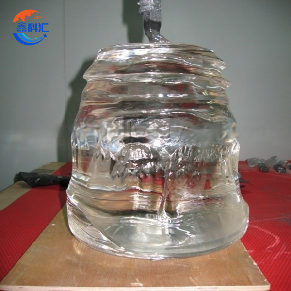
Optical Grade: UV laser windows (transmittance> 90%@200 nm)
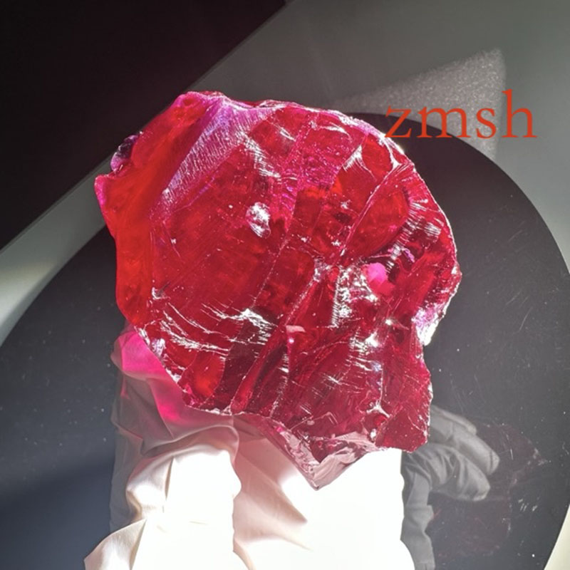
Mga Doped nga Variant: Ruby (konsentrasyon sa Cr³⁺ 0.01–0.5 wt.%), asul nga sapphire tubing
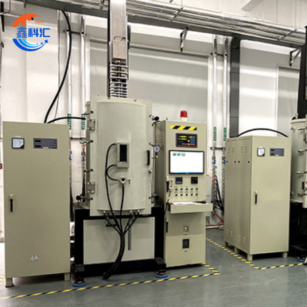
Kinauyokan nga mga sangkap sa Sistema
1. Sistema sa Pagtunaw
Iridium Crucible: Makasugakod sa 2300°C, makasugakod sa kaagnasan, nahiuyon sa dagkong pagkatunaw (100–400 kg).
Induction Heating Furnace: Multi-zone independent temperature control (±0.5°C), optimized thermal gradients.
2. Sistema sa Pagbira ug Pagtuyok
High-Precision Servo Motor: Pagbira nga resolusyon 0.01 mm/h, rotational concentricity <0.01 mm.
Magnetic Fluid Seal: Non-contact transmission para sa padayon nga pagtubo (>72 ka oras).
3. Thermal Control System
PID Closed-Loop Control: Real-time nga power adjustment (50–200 kW) aron mapalig-on ang thermal field.
Inert Gas Protection: Ar/N₂ mixture (99.999% purity) aron malikayan ang oksihenasyon.
4. Automation ug Monitoring
Pag-monitor sa Diameter sa CCD: Tinuod nga oras nga feedback (pagkatukma ± 0.01 mm).
Infrared Thermography: Pag-monitor sa solid-liquid interface morphology.
Pagtandi sa CZ batok sa KY Method
| Parameter | CZ nga pamaagi | Pamaagi sa KY |
| Max. Gidak-on sa Kristal | 12 ka pulgada (300 mm) | 400 mm (porma nga peras nga ingot) |
| Densidad sa depekto | <100/cm² | <50/cm² |
| Rate sa Pagtubo | 0.5–5 mm/h | 0.1–2 mm/h |
| Pagkonsumo sa Enerhiya | 50–80 kWh/kg | 80–120 kWh/kg |
| Mga aplikasyon | LED substrates, GaN epitaxy | Optical nga mga bintana, dagkong mga ingot |
| Gasto | Kasarangan (high equipment investment) | Taas (komplikado nga proseso) |
Pangunang mga Aplikasyon
1. Industriya sa Semiconductor
GaN Epitaxial Substrates: 2–8-pulgada nga mga wafer (TTV <10 μm) para sa Micro-LEDs ug laser diodes.
SOI Wafers: Ang pagkagapos sa nawong <0.2 nm alang sa 3D-integrated chips.
2. Optoelectronics
UV Laser Windows: Makasukol sa 200 W/cm² power density para sa lithography optics.
Infrared Components: Absorption coefficient <10⁻³ cm⁻¹ para sa thermal imaging.
3. Consumer Electronics
Mga Cover sa Camera sa Smartphone: Mohs nga katig-a 9, 10 × pag-uswag sa resistensya sa scratch.
Mga Display sa Smartwatch: Gibag-on 0.3–0.5 mm, transmittance> 92%.
4. Depensa ug Aerospace
Nuclear Reactor Windows: Radiation tolerance hangtod sa 10¹⁶ n/cm².
High-Power Laser Mirrors: Thermal deformation <λ/20@1064 nm.
Mga Serbisyo sa XKH
1. Pag-customize sa Kagamitan
Scalable Chamber Design: Φ200–400 mm configurations para sa 2–12-pulgada nga wafer production.
Flexibility sa Doping: Nagsuporta sa rare-earth (Er/Yb) ug transition-metal (Ti/Cr) doping para sa gipahaom nga optoelectronic nga mga kabtangan.
2. Katapusan nga Suporta
Pag-optimize sa Proseso: Pre-validated nga mga resipe (50+) alang sa LED, RF nga mga aparato, ug mga sangkap nga gipagahi sa radiation.
Global Service Network: 24/7 hilit nga diagnostics ug on-site maintenance nga adunay 24 ka bulan nga warranty.
3. Downstream nga Pagproseso
Wafer Fabrication: Paghiwa, paggaling, ug pagpasinaw alang sa 2-12-pulgada nga mga wafer (C/A-plane).
Mga Produkto nga Gidugang sa Bili:
Mga Optical nga Komponen: UV/IR nga mga bintana (0.5–50 mm ang gibag-on).
Mga Materyal nga Grade sa Alahas: Cr³⁺ ruby (GIA-certified), Ti³⁺ star sapphire.
4. Teknikal nga Pagpangulo
Mga Sertipikasyon: Mga wafer nga nagsunod sa EMI.
Mga patente: Mga core nga patente sa pagbag-o sa pamaagi sa CZ.
Panapos
Ang ekipo nga CZ method naghatod ug dako nga dimensyon nga compatibility, ultra-low defect rates, ug taas nga process stability, nga naghimo niini nga benchmark sa industriya alang sa LED, semiconductor, ug mga aplikasyon sa depensa. Ang XKH naghatag og komprehensibo nga suporta gikan sa pag-deploy sa mga ekipo ngadto sa pagproseso sa post-growth, nga makapahimo sa mga kliyente nga makab-ot ang cost-effective, high-performance sapphire crystal production.
May Kalabutan nga mga Produkto
-

Custom N Type SiC Seed Substrate Dia153/155mm F...
-

2pulgada 50.8mm Silicon wafer FZ N-Type SSP
-
Mga rubi/rubi nga hinimo sa lab para ibaligya Ruby# 5 Al2O3
-

SiC ceramic plate / tray alang sa 4inch 6inch wafer ho ...
-

12 Pulgada SiC substrate Diametro 300mm Gibag-on ...
-

GGG kristal nga sintetikong gemstone gadolinium galli...