Gipahaom nga SiC Seed Crystal Substrates Dia 205/203/208 4H-N nga Tipo para sa Optical Communications


Teknikal nga mga parametro
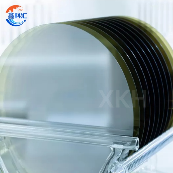
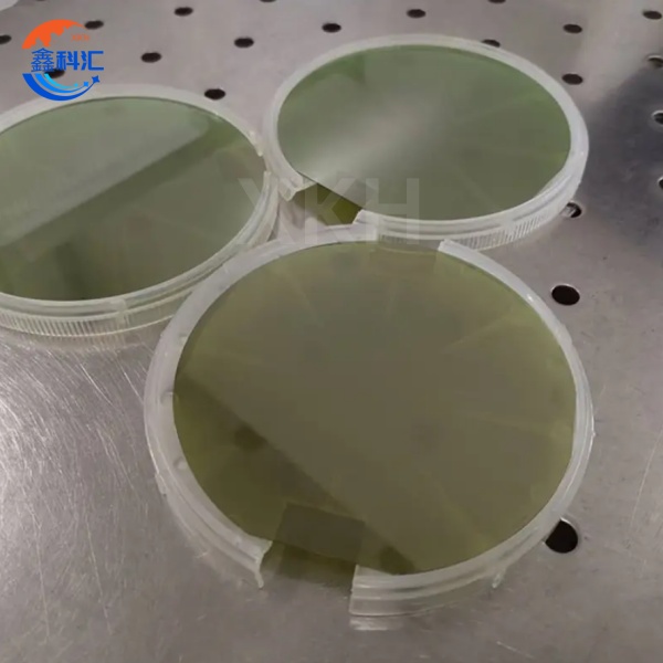
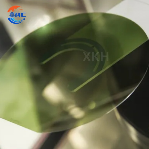
Wafer sa liso nga silicon carbide | |
Politipo | 4H |
Sayop sa oryentasyon sa nawong | 4° padulong sa<11-20>±0.5º |
Resistivity | pag-customize |
Diametro | 205±0.5mm |
Gibag-on | 600±50μm |
Kagaspang | CMP,Ra≤0.2nm |
Densidad sa Mikropipe | ≤1 matag usa/cm2 |
Mga garas | ≤5, Kinatibuk-ang Gitas-on ≤2 * Diametro |
Mga chips/indent sa ngilit | Wala |
Pagmarka sa laser sa atubangan | Wala |
Mga garas | ≤2, Kinatibuk-ang Gitas-on ≤Diametro |
Mga chips/indent sa ngilit | Wala |
Mga lugar nga polytype | Wala |
Pagmarka sa likod nga laser | 1mm (gikan sa ibabaw nga ngilit) |
Ngilit | Chamfer |
Pagputos | Multi-wafer cassette |
Pangunang mga Kinaiya
1. Istruktura sa Kristal ug Pagganap sa Elektrisidad
· Kalig-on sa Kristalograpiya: 100% 4H-SiC polytype dominance, walay multicrystalline inclusions (pananglitan, 6H/15R), nga adunay XRD rocking curve nga full-width sa half-maximum (FWHM) ≤32.7 arcsec.
· Taas nga Paglihok sa Carrier: Paglihok sa electron nga 5,400 cm²/V·s (4H-SiC) ug paglihok sa hole nga 380 cm²/V·s, nga nagtugot sa mga disenyo sa high-frequency device.
·Katig-a sa Radiasyon: Makasugakod sa 1 MeV neutron irradiation nga adunay displacement damage threshold nga 1×10¹⁵ n/cm², sulundon alang sa aerospace ug nukleyar nga mga aplikasyon.
2. Mga Kabtangan sa Thermal ug Mekanikal
· Talagsaong Thermal Conductivity: 4.9 W/cm·K (4H-SiC), triple sa silicon, nga mosuporta sa operasyon nga labaw sa 200°C.
· Ubos nga Thermal Expansion Coefficient: CTE nga 4.0×10⁻⁶/K (25–1000°C), nga nagsiguro sa pagkaangay sa silicon-based packaging ug pagminus sa thermal stress.
3. Pagkontrol sa Depekto ug Katukma sa Pagproseso
· Densidad sa Mikropipe: <0.3 cm⁻² (8-pulgada nga mga wafer), densidad sa dislokasyon <1,000 cm⁻² (gipamatud-an pinaagi sa KOH etching).
· Kalidad sa Nawong: Gipasinaw sa CMP ngadto sa Ra <0.2 nm, nga nakab-ot ang mga kinahanglanon sa pagkapatag nga grado sa EUV lithography.
Mga Pangunang Aplikasyon
| Dominyo | Mga Senaryo sa Aplikasyon | Teknikal nga mga Benepisyo |
| Komunikasyon sa Optika | 100G/400G nga mga laser, silicon photonics hybrid modules | Ang mga substrate sa liso sa InP nagpahimo sa direktang bandgap (1.34 eV) ug Si-based heteroepitaxy, nga nagpamenos sa optical coupling loss. |
| Bag-ong mga Sakyanan sa Enerhiya | 800V nga taas og boltahe nga mga inverter, mga onboard charger (OBC) | Ang 4H-SiC substrates makasugakod sa >1,200 V, nga makapakunhod sa conduction losses sa 50% ug system volume sa 40%. |
| 5G nga Komunikasyon | Mga aparato sa RF nga may balud sa milimetro (PA/LNA), mga power amplifier sa base station | Ang mga semi-insulating SiC substrates (resistivity >10⁵ Ω·cm) nagtugot sa high-frequency (60 GHz+) passive integration. |
| Mga Kagamitan sa Industriya | Mga sensor sa taas nga temperatura, mga transformer sa kuryente, mga monitor sa reaktor nukleyar | Ang mga substrate sa liso sa InSb (0.17 eV bandgap) naghatag og magnetic sensitivity hangtod sa 300%@10 T. |
Pangunang mga Bentaha
Ang SiC (silicon carbide) seed crystal substrates naghatag ug walay kapantay nga performance nga adunay 4.9 W/cm·K thermal conductivity, 2–4 MV/cm breakdown field strength, ug 3.2 eV wide bandgap, nga makapahimo sa high-power, high-frequency, ug high-temperature applications. Nga adunay zero micropipe density ug <1,000 cm⁻² dislocation density, kini nga mga substrate nagsiguro sa kasaligan sa grabeng mga kondisyon. Ang ilang chemical inertness ug CVD-compatible surfaces (Ra <0.2 nm) nagsuporta sa advanced heteroepitaxial growth (pananglitan, SiC-on-Si) para sa optoelectronics ug EV power systems.
Mga Serbisyo sa XKH:
1. Gipahaom nga Produksyon
· Mga Pormat sa Flexible nga Wafer: 2–12-pulgada nga mga wafer nga adunay lingin, rektanggulo, o gipahaom nga porma nga mga hiwa (±0.01 mm nga tolerance).
· Pagkontrol sa Doping: Tukma nga pag-doping sa nitroheno (N) ug aluminum (Al) pinaagi sa CVD, nga makab-ot ang resistivity gikan sa 10⁻³ hangtod 10⁶ Ω·cm.
2. Abansadong mga Teknolohiya sa Proseso"
· Heteroepitaxy: SiC-on-Si (compatible sa 8-pulgada nga silicon lines) ug SiC-on-Diamond (thermal conductivity >2,000 W/m·K).
· Pagpamenos sa Depekto: Hydrogen etching ug annealing aron makunhuran ang mga depekto sa micropipe/density, nga makapauswag sa wafer yield ngadto sa >95%.
3. Mga Sistema sa Pagdumala sa Kalidad"
· End-to-End nga Pagsulay: Raman spectroscopy (polytype verification), XRD (crystallinity), ug SEM (defect analysis).
· Mga Sertipikasyon: Nakasunod sa AEC-Q101 (awtomatikong kagamitan), JEDEC (JEDEC-033), ug MIL-PRF-38534 (klase militar).
4. Suporta sa Kadena sa Suplay sa Tibuok Kalibutan"
· Kapasidad sa Produksyon: Binulan nga output >10,000 ka wafer (60% 8-pulgada), nga adunay 48-oras nga emerhensya nga paghatud.
· Logistics Network: Sakop sa Europe, North America, ug Asia-Pacific pinaagi sa air/sea freight nga adunay temperature-controlled packaging.
5. Teknikal nga Pag-uswag"
· Hiniusang mga Laboratoryo sa R&D: Nagtinabangay sa pag-optimize sa pagputos sa SiC power module (pananglitan, paghiusa sa DBC substrate).
· Paglilisensya sa IP: Paghatag og lisensya sa teknolohiya sa pagtubo sa epitaxial sa GaN-on-SiC RF aron makunhuran ang gasto sa R&D sa kliyente.
Sumaryo
Ang mga substrate sa SiC (silicon carbide) seed crystal, isip usa ka estratehikong materyal, nag-usab sa paghulma sa mga kadena sa industriya sa kalibutan pinaagi sa mga kalampusan sa pagtubo sa kristal, pagkontrol sa depekto, ug heterogeneous integration. Pinaagi sa padayon nga pag-uswag sa pagkunhod sa depekto sa wafer, pag-scale sa 8-pulgada nga produksiyon, ug pagpalapad sa mga plataporma sa heteroepitaxial (pananglitan, SiC-on-Diamond), ang XKH naghatag og taas nga kasaligan, epektibo sa gasto nga mga solusyon alang sa optoelectronics, bag-ong enerhiya, ug abante nga paggama. Ang among pasalig sa kabag-ohan nagsiguro nga ang mga kliyente nanguna sa carbon neutrality ug intelihenteng mga sistema, nga nagduso sa sunod nga panahon sa lapad nga bandgap semiconductor ecosystems.
Mga May Kalabutan nga Produkto
-

150mm 6 pulgada 0.7mm 0.5mm nga Sapphire Wafer Substra...
-

Silicon Carbide Cantilever Paddle (SiC Cantilev...
-

156mm 159mm 6 pulgada nga Sapphire Wafer para sa carrier C...
-
Berde nga sapiro para sa mutya nga berde nga olibo nga artipisyal...
-

p-type 4H/6H-P 3C-N TYPE SIC substrate 4 pulgada ...
-

Mga LiTaO3 Lithium Tantalate Ingots nga adunay Fe/Mg Dopi...